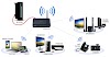
A printed circuit board, or PCB, is used to mechanically support and electrically connect electronic components using conductive pathways, tracks or signal traces etched from copper sheets laminated onto a non-conductive substrate. It is also referred to as printed wiring board (PWB) or etched wiring board. A PCB populated with electronic components is a printed circuit assembly (PCA), also known as a printed circuit board assembly or PCB Assembly (PCBA). Printed circuit boards are used in virtually all but the simplest commercially produced electronic devices.
Alternatives to PCBs include wire wrap and point-to-point construction. PCBs are often less expensive and more reliable than these alternatives, though they require more layout effort and higher initial cost. PCBs are much cheaper and faster for high-volume production since production and soldering of PCBs can be done by automated equipment. Much of the electronics industry's PCB design, assembly, and quality control needs are set by standards that are published by the IPC organization.

Development of the methods used in modern printed circuit boards started early in the 20th century. In 1903, a German inventor, Albert Hanson, described flat foil conductors laminated to an insulating board, in multiple layers. Thomas Edison experimented with chemical methods of plating conductors onto linen paper in 1904. Arthur Berry in 1913 patented a print-and-etch method in Britain, and in the United States Max Schoop obtained a patent[1] to flame-spray metal onto a board through a patterned mask. Charles Durcase in 1927 patented a method of electroplating circuit patterns. [2]
The Austrian Jewish engineer Paul Eisler invented the printed circuit while working in England around 1936 as part of a radio set. Around 1943 the USA began to use the technology on a large scale to make proximity fuses for use in World War II [2]. After the war, in 1948, the USA released the invention for commercial use. Printed circuits did not become commonplace in consumer electronics until the mid-1950s, after the Auto-Sembly process was developed by the United States Army.
Before printed circuits (and for a while after their invention), point-to-point construction was used. For prototypes, or small production runs, wire wrap or turret board can be more efficient. Predating the printed circuit invention, and similar in spirit, was John Sargrove's 1936–1947 Electronic Circuit Making Equipment (ECME) which sprayed metal onto a Bakelite plastic board. The ECME could produce 3 radios per minute.
During World War II, the development of the anti-aircraft proximity fuse required an electronic circuit that could withstand being fired from a gun, and could be produced in quantity. The Centralab Division of Globe Union submitted a proposal which met the requirements: a ceramic plate would be screenprinted with metallic paint for conductors and carbon material for resistors, with ceramic disc capacitors and subminiature vacuum tubes soldered in place.[3]
Originally, every electronic component had wire leads, and the PCB had holes drilled for each wire of each component. The components' leads were then passed through the holes and soldered to the PCB trace. This method of assembly is called through-hole construction. In 1949, Moe Abramson and Stanislaus F. Danko of the United States Army Signal Corps developed the Auto-Sembly process in which component leads were inserted into a copper foil interconnection pattern and dip soldered. The patent they obtained in 1956 was assigned to the U.S. Army. [4] With the development of board lamination and etching techniques, this concept evolved into the standard printed circuit board fabrication process in use today. Soldering could be done automatically by passing the board over a ripple, or wave, of molten solder in a wave-soldering machine. However, the wires and holes are wasteful since drilling holes is expensive and the protruding wires are merely cut off.
In recent years, the use of surface mount parts has gained popularity as the demand for smaller electronics packaging and greater functionality has grown.


